PCBSKY

Blind- und Buried-Via Leiterplatte (HDI PCB)

Blind and buried via printed circuit boards (BPCBs) are an advanced HDI technology that enables internal connections between different PCB layers. They are used for high-density, compact, and high-performance electronic designs.

Original price was: ¥49.50.Current price is: ¥39.50.

Add to quote

Langbeschreibung

overview

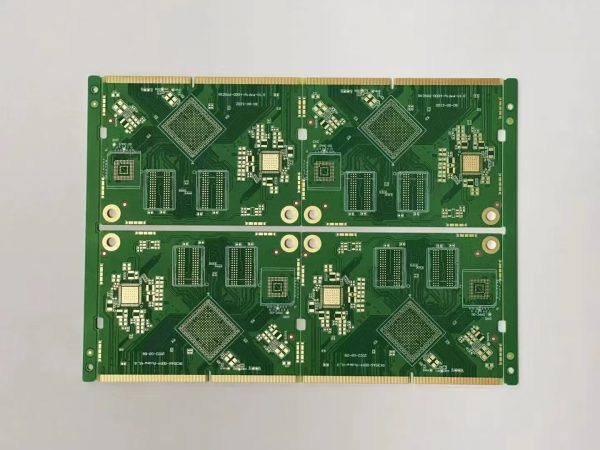
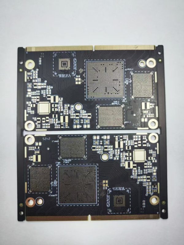
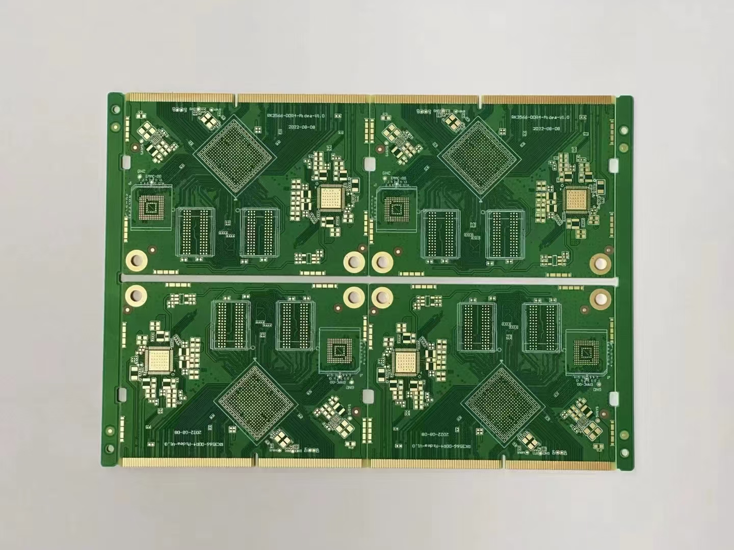
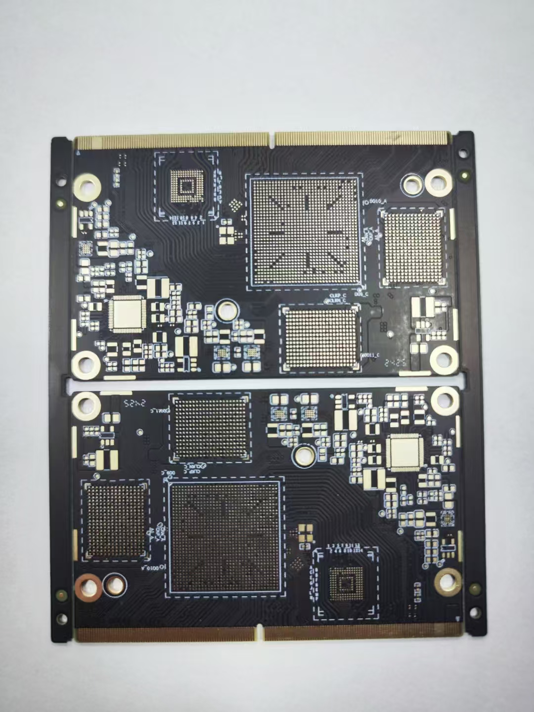
Blind and buried vias are a key technology in modern HDI printed circuit boards. They enable electrical connections between inner and outer layers without penetrating the entire circuit board. This results in higher circuit density and improved electrical performance.

At PCBSky, we manufacture high-quality HDI printed circuit boards with precise via technology for complex and highly integrated electronic applications.


Key features:

  • Blind via connections (outer layer → inner layer)
  • Buried-Via Connections (Inner Layers Only)
  • High wiring density for complex designs
  • Improved signal integrity
  • Reduced PCB size and weight
  • Ideal for high-speed electronics

Manufacturing technology at PCBSky:

Our production uses modern processes:

  • Laser drilling technology for micro-vias
  • Precise layer alignment
  • Automated Optical Inspection (AOI)
  • Electrical tests before shipping
  • Strict quality control

Applications:

  • Smartphones & Tablets
  • 5G communication systems
  • High-performance computers
  • Medical technology
  • Aerospace Electronics
  • Industrial control systems

Why PCBSky HDI Technology:

  • High-precision via manufacturing
  • Reliable multi-layer structures
  • Support for complex HDI designs
  • Fast production & delivery
  • Suitable for prototype and series production

Verwandte Produkte

Die PTFE-Leiterplatte ist eine Hochfrequenz-Printed Circuit Board Lösung, die aus Polytetrafluorethylen (PTFE) Material hergestellt wird. Sie bietet extrem niedrige Signalverluste, hohe thermische Stabilität und hervorragende elektrische Eigenschaften für anspruchsvolle RF- und Hochgeschwindigkeitsanwendungen.

The high-frequency printed circuit board (PCB) is a specialized PCB solution for high-frequency and fast signal transmission. It is manufactured using high-quality materials such as PTFE or special high-frequency laminates and offers minimal signal loss as well as excellent electrical performance.

Blind and buried via printed circuit boards (BPCBs) are an advanced HDI technology that enables internal connections between different PCB layers. They are used for high-density, compact, and high-performance electronic designs.

Die Dickkupfer-Leiterplatte ist eine spezielle Leiterplatte mit stark erhöhtem Kupfergewicht, die für hohe Strombelastung, Wärmeableitung und industrielle Anwendungen entwickelt wurde. Sie bietet hervorragende Zuverlässigkeit für leistungsstarke elektronische Systeme.

Scroll to Top